

SiTrans
Förderkennzeichen: 49MF220054
Projektlaufzeit: 01.09.2022 bis 31.10.2024
Laser welding of silicon in the transparency range
Development goal
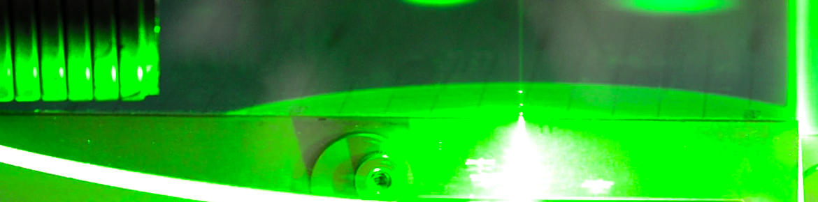
The goal of the development was to investigate a new method for joining silicon with minimal heat exposure. Silicon is the key material in the semiconductor industry and is found in almost all microelectronic products. There are established methods for joining silicon with other materials, but these involve high overall thermal stress. This can significantly limit the precision and flexibility of further functionalization and miniaturization of components. In semiconductor manufacturing, sensor technology, and microsystems technology in particular, there is a constant interest in utilizing higher integration densities and more complex component architectures. The project therefore investigated the transmissive joining of silicon using a newly developed ultrashort pulse laser system. The approach aims to apply the laser energy through the silicon in a targeted manner at the interface with another joining partner – without subjecting the component as a whole to thermal stress.
Advantages and solutions
The project used a newly developed ultrashort pulse laser system (UKP) with a wavelength of 2 µm to investigate an innovative method for joining silicon with another material partner. The key advantage of this approach is that silicon is partially transparent at this wavelength, meaning that the laser beam can penetrate the silicon and act specifically on the joining zone. The energy is concentrated so intensely at the laser's focal point that high absorption occurs there. This makes it possible to generate local changes at the interface between the materials, even to the point of melting. Due to the extremely short pulses of the laser, the thermal load remains very limited in terms of space, which protects the surrounding structures. A particular focus was placed on investigating how much energy can actually be introduced into the joining zone through the silicon. This is because silicon exhibits complex, so-called nonlinear effects during this type of processing, which greatly influence the effectiveness of the energy input. As part of the project, extensive tests on laser-material interaction were therefore carried out. These included optimizing sample preparation, precise control of the process, and systematic test series under various conditions. The aim was to precisely determine the technical limits and potential of this novel joining process.
Target market
The findings obtained in the project are primarily aimed at research institutions and development departments in the semiconductor processing industry. Since the process is not yet available as a reliable series production process, the focus is on testing, further development, and application in the context of technological feasibility studies, prototype development, and R&D projects. A planned knowledge transfer will take place via established networks and topic-specific specialist events, which will enable targeted discussion of the results and their further development. Close communication with the manufacturer of the laser system will allow the limitations and requirements identified in the project to be communicated directly for the optimization and adaptation of the system to specific process requirements. In addition, the project strengthens the technical expertise of ifw Jena in the field of ultra-short pulse laser applications and forms the basis for new R&D collaborations. Interested partners from industry and research will have the opportunity to use the novel laser system for their own research questions, enabling potential applications to be identified at an early stage and jointly developed.